
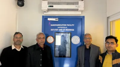
Uttarakhand's First Nanofabrication Facility: A Leap in Semiconductor Manufacturing
| Aspect | Details |
|---|---|
| Event | Establishment of Uttarakhand's First Nanofabrication Facility |
| Location | IIT-Roorkee, Uttarakhand |
| Collaboration | - International: Taiwan's premier semiconductor institutions |
| - Domestic: Funded by the Department of Science and Technology (DST) | |
| Project Start Year | 2019 |
| Key Infrastructure | - 50 kV Electron Beam Lithography (EBL) system with 10nm resolution |
| - Inductively Coupled Plasma RIE (ICP-RIE) | |
| - Ultra-clean rooms: Class 100 space (300 sq ft) and Class 1000 space (600 sq ft) | |
| Research Applications | - Quantum sensors, Spintronics, Memory devices, Thin-film devices, Photodetectors, Quantum optics, Photonic crystals |
| About DST | - Founded on 3rd May 1971 |
| - Functions: Funding, policy-making, international scientific coordination | |
| - Supports scientists, institutions, and stakeholders in Science & Technology | |
| - DST's budget has increased by 100% over the years, enabling new initiatives |